Next Generation Quantum Chips
Faster. All silicon. Atomic scale. Energy efficient. Room temperature operation.
At QSi we develop the world's first practical implementation of field controlled computing. QSi devices compute without transistors by rearranging a fixed collection of electrons. This is practical, very fast, and very energy-efficient.
Our atomic-scale, ultra-low-power field controlled computing is based on unique single-atom Silicon Quantum Dots.
Our devices are orders of magnitude faster than the best CMOS devices, but fully compatible with them on the same chip.
Quantum Accelerator Chips: Tiny, fast, and cool
QSi is changing the face of computing. We have created the first practical implementation of an atomic scale architecture that does not use transistors.
Why does that matter? Ordinary computer circuits pump enormous numbers of electrons with each cycle of the clock. Then all those electrons are dumped as heat. It is extremely expensive to get rid of all that heat. That has forced an end to the Moore’s Law path that has driven the semiconductor industry for the past half century. So computers are not getting any faster. It takes a lot of energy to run them. That energy is largely wasted. QSi has shown that it doesn’t have to be that way.
How do we do it? The Quantum Silicon approach harnesses our easy access to quantum phenomena in collections of silicon atoms to represent, transmit, and create information. Our process uses virtually no current. The result is a new generation of quantum accelerators that are tiny, fast, and cool.
• All-silicon - allowing integration into today’s architecture
• Room temperature operation
• 100X less power consumed than the best of today’s technology
Team
QSi has assembled a small, expert team of developers and entrepreneurs
Ken Gordon - CEO
Robert A. Wolkow - CTO
Jason Pitters - NRC Collaborator
Ryan Foote - Univ of Sherbrooke Collaborator
Lucian Livadaru - Development Scientist
Roshan Achal - Development Scientist
Jeremiah Croshaw - Development Scientist
Brad Hesson - Development Scientist

Contact

Quantum Silicon Inc.
11421 Saskatchewan Drive
Edmonton, Alberta
Canada T6G 2M9
Ken Gordon CEO +1 (780) 641-1963
News / Publications


Scalable Atomically Precise Manufacturing
In 1989 Don Eigler at IBM’s Almaden Research Center showed how to use a Scanning Probe Microscope (SPM) to position individual atoms. IBM at the time predicted that the technique might one day be used to build atom-scale transistors that would be faster than what was available then. Now, over 30 years later, QSi is leading the world in developing and using atomically precise manufacturing to create electronics that use no transistors, are far faster than their transistor-based equivalent, and consume orders of magnitude less energy.

September 22, 2022


Deep learning-guided surface characterization for autonomous hydrogen lithography
As the development of atom scale devices transitions from novel, proof-of-concept demonstrations to state-of-the-art commercial applications, automated assembly of such devices must be implemented. Here we present an automation method for the identification of defects prior to atomic fabrication via hydrogen lithography using deep learning. We trained a convolutional neural network to locate and differentiate between surface features of the technologically relevant hydrogen-terminated silicon surface imaged using a scanning tunneling microscope. Once the positions and types of surface features are determined, the predefined atomic structures are patterned in a defect-free area. By training the network to differentiate between common defects we are able to avoid charged defects as well as edges of the patterning terraces. Augmentation with previously developed autonomous tip shaping and patterning modules allows for atomic scale lithography with minimal user intervention.

March 18, 2020

Detecting and Directing Single Molecule Binding Events on H-Si(100) with Application to Ultradense Data Storage
Many diverse material systems are being explored to enable smaller, more capable and energy efficient devices. These bottom up approaches for atomic and molecular electronics, quantum computation, and data storage all rely on a well-developed understanding of materials at the atomic scale. Here, we report a versatile scanning tunneling microscope (STM) charge characterization technique, which reduces the influence of the typically perturbative STM tip field, to develop this understanding even further. Using this technique, we can now observe single molecule binding events to atomically defined reactive sites (fabricated on a hydrogen-terminated silicon surface) through electronic detection. We then developed a simplified error correction tool for automated hydrogen lithography, quickly directing molecular hydrogen binding events using these sites to precisely repassivate surface dangling bonds (without the use of a scanned probe). We additionally incorporated this molecular repassivation technique as the primary rewriting mechanism in ultradense atomic data storage designs (0.88 petabits per in2).

November 27, 2019
Electrostatic Landscape of a Hydrogen-Terminated Silicon Surface Probed by a Moveable Quantum Dot
With nanoelectronics reaching the limit of atom-sized devices, it has become critical to examine how irregularities in the local environment can affect device functionality. Here, we characterize the influence of charged atomic species on the electrostatic potential of a semiconductor surface at the subnanometer scale. Using noncontact atomic force microscopy, two-dimensional maps of the contact potential difference are used to show the spatially varying electrostatic potential on the (100) surface of hydrogen-terminated highly doped silicon. Three types of charged species, one on the surface and two within the bulk, are examined. An electric field sensitive spectroscopic signature of a single probe atom reports on nearby charged species. The identity of one of the near-surface species has been uncertain in the literature, and we suggest that its character is more consistent with either a negatively charged interstitial hydrogen or a hydrogen vacancy complex.

August 6, 2019

Binary Atomic Silicon Logic
It has been proposed that miniature circuitry will ultimately be crafted from single atoms. Despite many advances in the study of atoms and molecules on surfaces using scanning probe microscopes, challenges with patterning and limited thermal structural stability have remained. Here we demonstrate rudimentary circuit elements through the patterning of dangling bonds on a hydrogen-terminated silicon surface. Dangling bonds sequester electrons both spatially and energetically in the bulk bandgap, circumventing short-circuiting by the substrate. We deploy paired dangling bonds occupied by one moveable electron to form a binary electronic building block. Inspired by earlier quantum dot-based approaches, binary information is encoded in the electron position, allowing demonstration of a binary wire and an OR gate.

December 13, 2018
_JPG.jpg)

Lithography for robust and editable atomic-scale silicon devices and memories
At the atomic scale, there has always been a trade-off between the ease of fabrication of structures and their thermal stability. Complex structures that are created effortlessly often disorder above cryogenic conditions. Conversely, systems with high thermal stability do not generally permit the same degree of complex manipulations. Here, we report scanning tunneling microscope (STM) techniques to substantially improve automated hydrogen lithography (HL) on silicon, and to transform state-of-the-art hydrogen repassivation into an efficient, accessible error correction/editing tool relative to existing chemical and mechanical methods. These techniques are readily adapted to many STMs, together enabling fabrication of error-free, room-temperature stable structures of unprecedented size. We created two rewriteable atomic memories (1.1 petabits per in2), storing the alphabet letter-by-letter in 8 bits and a piece of music in 192 bits. With HL no longer faced with this trade-off, practical silicon-based atomic-scale devices are poised to make rapid advances towards their full potential.
.jpg)
July 23, 2018
Atomic White Out
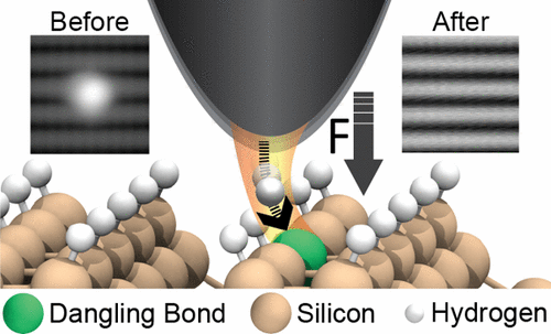
Although patterning of atomic silicon quantum dots (ASiQDs) to create nanoelectronic devices has been possible for some years, even the best patterning technique has been susceptible to occasional error. This paper demonstrates the mechanochemistry bonding of a single hydrogen atom to a ASiQD or erase or “passivate” it, opening the door for larger and more elaborate ASiQD structures and furthering scalability of the paradigm.
July 18, 2017